生產能力


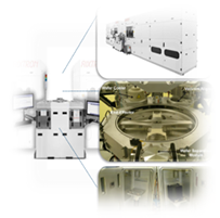
Capabilities of GaN CVD System


  • Full automation wafer transfer system to reduce the particles added during wafer load/unload.
  • High material uniformity of GaN HEMT up-to 200 mm epitaxy wafer
  • In-situ reactor clean concept to avoid substrate contamination during epitaxial growth.
  • High throughput C2C platform with 1500 pcs of 650V wafers per month.


Capabilities of SiC CVD System


  • Single wafer, dual reactor with auto wafer transfer system reduce the particles added during wafer load/unload.
  • High cross-wafer epi-thickness & doping uniformity on 4”~ 8” SiC epitaxial wafers.
  • Rapid heat up/cooling down with high rpm rotation reactor design, provide the capacity of 2K/month of 6um ultra low Killer defect epi-wafer.